Reducing Environmental Impact
At Kioxia Group, we are committed to achieving both efficient manufacturing and reducing the environmental impact of our complex semiconductor manufacturing processes. We recycle the substantial amounts of daily waste we produce, with a particular focus on maintaining a high recycling rate for plastic waste.
Additionally, we continue striving to reduce CO2 emissions from packaging materials used for transporting wafers, products, and semi-finished goods.
Aiming for a Resource-Saving Manufacturing Facility
Kioxia Iwate Corporation’s Fab2 (“K2”) was completed in 2024. It incorporates the environmental technologies that Kioxia Group has accumulated to date, and is designed to mitigate and adapt in response to climate change.
Wastewater treatment was conventionally carried out by passing wastewater from the manufacturing process through a relay tank installed in the basement below the fab, before being piped to an outdoor wastewater treatment facility. For the K2 fab, we have used the difference in ground elevation between the fab and the wastewater treatment facility to create a system that uses gravity to directly pass wastewater from the manufacturing line to the treatment facility.
This design removes the need for 70 tanks and over 100 pumps,1 while reducing electric power required for pump operation. Furthermore, since it is not necessary to provide a basement for installation of pumps, the facility eliminates the need for around 14,000 m3 of concrete and approximately 2,000 tons of rebar, effectively reducing the use of resources that have a high carbon concentration.
1 Comparing the K2 building with Kioxia Iwate Corporation’s Fab1 building, which is of the same size
Efforts to Reduce Resource Usage in the Manufacturing Process
We use nozzles to apply chemicals providing protective coatings on wafer surfaces. It is necessary to regularly clean the nozzles with organic solvents to prevent discharge failures caused by chemical solidification. At Kioxia Corporation's Yokkaichi Plant, the optimization of nozzle cleaning frequency has reduced the usage of organic solvents for cleaning by over 40% in some processes.
Additionally, a review of the chemical usage and the order of processes during wafer cleaning has resulted in reduced water consumption and stabilized product quality. By increasing the recovery rate and reusing chemicals, we have reduced their usage by around 50% in some processes.
Extending Resource Lifespan through Manufacturing Equipment Maintenance
The maintenance of manufacturing equipment is crucial for ensuring a balance between maintaining a product’s quality and reducing its environmental impact.
Some of the equipment used in back-end processes at Kioxia Corporation's Yokkaichi Plant has been in use for a long time, making the improvement of maintenance efficiency a challenge. To address this, the plant's Reuse Workshop has been looking at ways to reuse parts. For consumable parts, the plant spent two years determining the types of wear that do not affect the operation of the equipment, revising the disposal criteria for these components, and doubling their usage period. Additionally, equipment and parts removed due to defects are disassembled, the faulty areas and causes are identified, and repairs carried out and the items re-used wherever possible. The quality of repairs and reuse is ensured through the careful use of data sourced from repair histories and inspections using in-house function checkers, contributing to improved maintenance efficiency. Since its inception in 2013, the workshop has been able to re-use approximately 54,000 parts as a result of these initiatives.
In the front-end process, also known as the circuit formation process, we focused on the surface degradation of the electrostatic chucks used to secure wafers to the equipment. Previously, these chucks were discarded after a certain number of uses, but since 2023, they have been reused as a result of enhanced maintenance processes. When circuit patterns are etched onto wafers (a multi-stage process using gas and plasma), the required precision varies in accordance with the stage of processing, and this allows us to determine whether recycled electrodes can be used. Our focus on this enables us to extend the usable life of electrodes and reduce the use of new ones by approximately 20%.
Recycling and Reuse of Waste Generated during Manufacturing
At Kioxia Group’s manufacturing sites, we are constantly making efforts to utilize resources more efficiently. With reuse and recycling as our top priorities, we sort materials on the premises by type and intended use after reprocessing.
*Table can be scrolled horizontally.
| Manufacturing Sites in Japan | Applications after Recycling | |
|---|---|---|
| Sources of Emissions | Waste (excluding plastics) | |
| Abatement equipment | Sludge | Rare metal raw materials |
| Wastewater treatment | Sludge | Cement raw materials |
| Manufacturing processes (circuit formation, wafer cleaning, etc.) | Waste oil | Organic solvents |
| Waste acids | Chemical raw materials, fertilizer raw materials | |
| Waste alkalis | Denitrification agents and combustion aids for boilers, chemical raw materials | |
| Packaging materials for new manufacturing equipment, replaced consumables | Metals | Metal raw materials |
During the aforementioned use of organic solvent for nozzle cleaning, not only is the entire amount of used organic solvent collected, but through a purification process carried out at a partner company, it is now possible to recycle most of it. The recycling rate of this organic solvent is 85%.
Efforts to generate recycled aluminum from aluminum laminate bags used as raw material packaging have been initiated at Solid State Storage Technology Corporation (SSSTC), and in 2024, 1.5 tons of aluminum laminate bags were recycled.
Effective Utilization of Plastic Waste
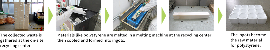
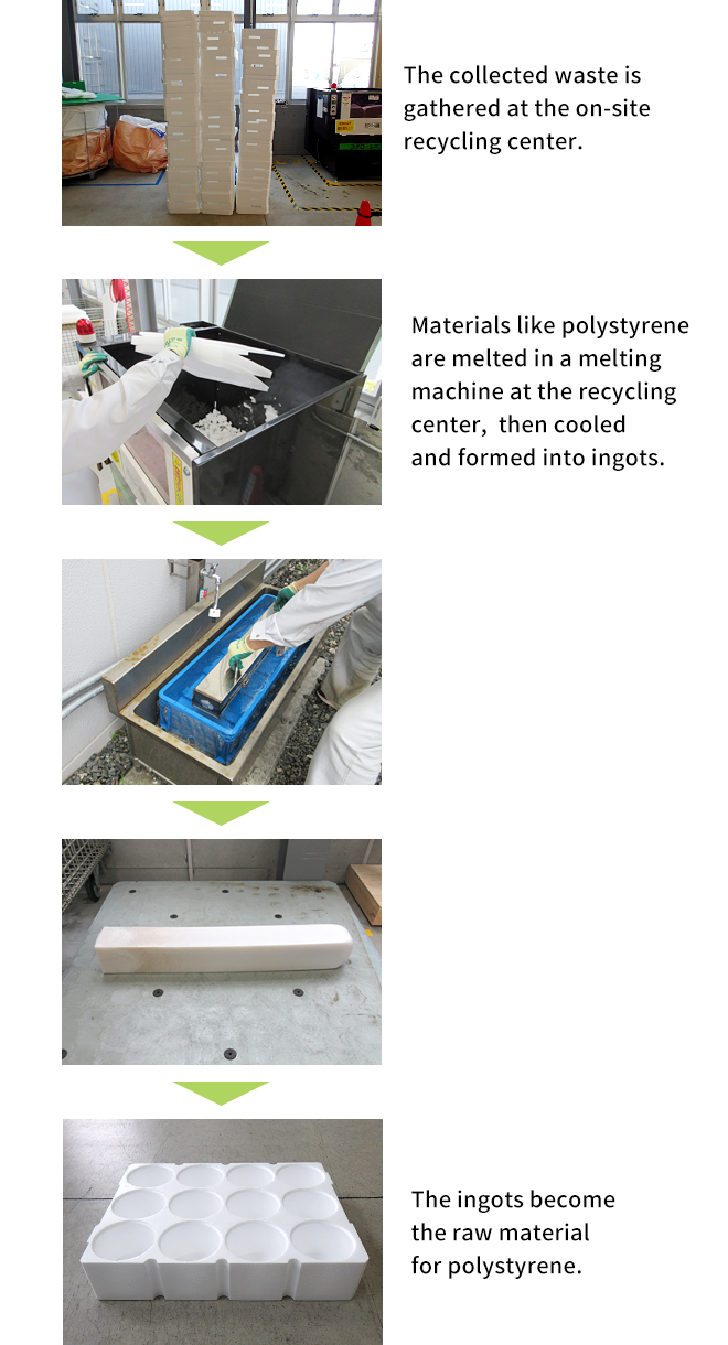
Over 2,000 tons of plastic waste are generated annually at Kioxia Group’s manufacturing sites in Japan. In collaboration with recycling companies, this waste is recycled into raw materials for plastic products and other uses. To improve the efficiency of recycling and transportation, thorough separation and collection are implemented, and the volume of plastic waste is reduced wherever possible. For instance, the volume of polystyrene waste is reduced by more than 95% through high-temperature melting.
As a result of these efforts, the recycling rate for plastic waste from domestic manufacturing facilities has consistently remained above 90% since FY2018.
Additionally, SSSTC has been reusing all of the trays used to transport memory products, amounting to 4.5 tons reused in FY2024.
Recycling Rate for Plastic Waste
from Domestic Manufacturing Facilities (%)
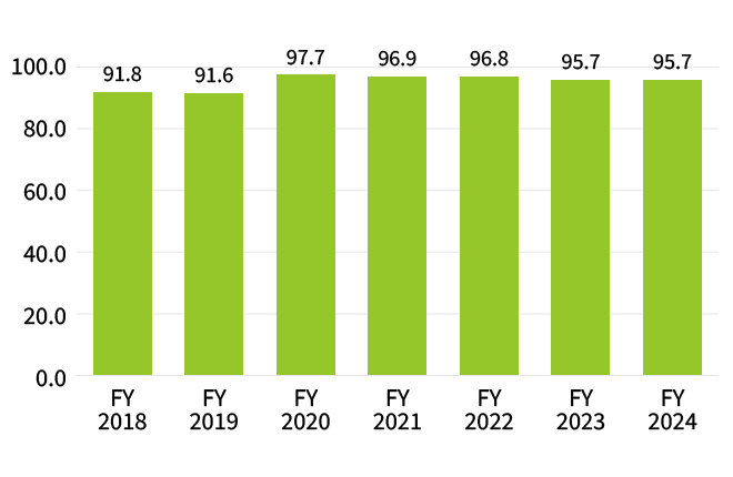
*Table can be scrolled horizontally.
| Manufacturing Sites in Japan | Outside Recycling Contractor | Applications after Recycling | |
|---|---|---|---|
| Types of Plastic Product Waste | Materials Sorted | ||
|
|
|
|
Example
Use of Environmentally Conscious Packaging
Kioxia Group is expanding its use of environmentally conscious packaging. Memory chips and silicon wafers are transported between our sites and those of subcontractors or material suppliers during manufacturing and processing. To maintain the quality of these delicate components, we use durable plastic cases that provide effective protection during transportation and ensure cleanliness. Kioxia Group in Japan inspects and recycles these cases after use.
We have adopted the use of paper trays for some of our consumer SSD products. The EXCERIA PLUS G3 NVMe™ and EXCERIA PLUS G4 NVMe™ use cardboard trays.2 We also use molded pulp trays for EXCERIA PLUS Portable SSDs and cardboard trays for our EXCERIA with Heatsink product.
Additionally, over 95% of the printed cardboard used at Kioxia Corporation's Yokkaichi Plant contains plant-based ingredients in its ink,3 reducing CO2 emissions by approximately 2% per unit of printing.
- 2 For each EXCERIA PLUS G3 NVMe™ product, the weight of plastic used in the packaging has been reduced by over 90% compared to the EXCERIA PLUS G2 NVMe™, which used plastic trays.
- 3 More than 10% of the ink solids comprise plant-based ingredients.
Note: NVMe is a registered or unregistered trademark of NVM Express, Inc. in the United States and other countries.